


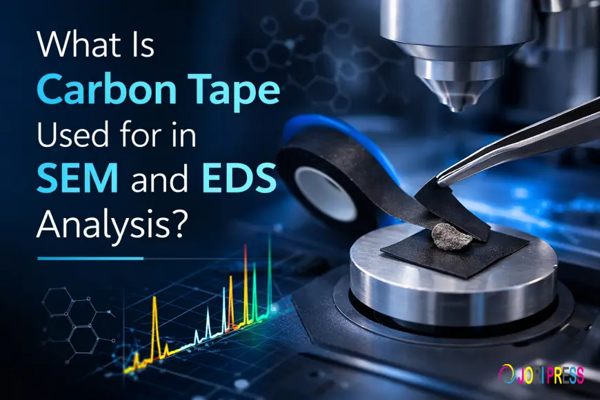
What Is Carbon Tape Used for in SEM and EDS Analysis
Carbon Tape for SEM is widely used in SEM and EDS analysis to mount samples, improve conductivity, and ensure stable imaging during electron microscopy testing.
In modern scientific research, particularly in materials science, nanotechnology, and electronics, high-resolution imaging and accurate elemental analysis are essential. Techniques like Scanning Electron Microscopy (SEM) and Energy Dispersive X-ray Spectroscopy (EDS) allow scientists to study the microstructure and composition of materials in incredible detail. However, the accuracy of these techniques is heavily dependent on proper sample preparation.
One of the most commonly used consumables for sample preparation is carbon tape. Despite its simplicity, carbon tape plays a critical role in ensuring reliable results during SEM and EDS analysis. In this article, we’ll dive deep into what carbon tape is, how it works, and why it’s indispensable in electron microscopy and elemental analysis.
What Is Carbon Tape?
Carbon tape is a double-sided adhesive tape coated with conductive carbon material. It is specially designed for laboratory applications where electrical conductivity, stable sample mounting, and minimal interference are crucial. Unlike ordinary adhesive tapes, carbon tape is engineered to withstand the vacuum conditions inside an SEM and provide a conductive pathway for electrons.
Key properties of carbon tape include:
-
Electrical conductivity: Prevents charging effects in non-conductive samples.
-
Strong adhesion: Holds samples securely during imaging.
-
Low contamination: Minimizes interference with analytical data.
-
Vacuum compatibility: Can withstand SEM vacuum without outgassing.
-
Uniform thickness: Provides a consistent base for accurate imaging.
In essence, carbon tape is both a mounting medium and a conductor, making it indispensable for SEM and EDS workflows.
The Role of Carbon Tape in SEM Analysis
A Scanning Electron Microscope (SEM) produces images by scanning a focused electron beam across a sample’s surface. These electrons interact with the atoms in the sample to produce signals that reveal surface morphology, texture, and topography.
However, non-conductive samples, like polymers, ceramics, or biological specimens, tend to accumulate electrons on their surface, a phenomenon known as electron charging. This causes image artifacts such as bright spots, streaking, and blurred areas, reducing the quality of the data. Carbon tape addresses this problem in multiple ways:
1. Secure Sample Mounting
Carbon tape allows researchers to firmly attach samples to SEM stubs or holders, preventing movement during imaging. Since SEM analysis often occurs under high vacuum conditions, even slight sample displacement can compromise results. Carbon tape ensures mechanical stability.
2. Electrical Conductivity
The carbon coating provides a conductive path for electrons to flow from the sample to the stub, which prevents surface charging. This is particularly important for non-metallic or low-conductivity materials, ensuring clear, high-resolution images.
3. Reducing Image Artifacts
By minimizing charging, carbon tape helps reduce common SEM artifacts, including:
-
Bright spots caused by local charging
-
Shadowing effects on the sample surface
-
Image drift during high-magnification scans
This ensures accurate representation of surface features, which is crucial for quantitative SEM analysis.
The Role of Carbon Tape in EDS Analysis
Energy Dispersive X-ray Spectroscopy (EDS) is often used alongside SEM to analyze a sample’s elemental composition. In EDS, an electron beam excites atoms in the sample, causing them to emit characteristic X-rays, which reveal the presence and quantity of elements.
Carbon tape plays an essential role in ensuring reliable EDS measurements:
1. Minimal Elemental Interference
Because carbon is a light element, it produces very low X-ray signals in EDS. This minimizes interference with the sample’s elemental spectrum, allowing accurate detection of elements like metals, oxides, and semiconductors.
2. Stable Sample Positioning
A securely mounted sample reduces positional shifts during EDS scanning, which is crucial for accurate mapping of elemental distribution across a sample’s surface.
3. Conductivity Benefits
Just like in SEM imaging, the conductive property of carbon tape ensures electron flow, reducing charging that could distort EDS measurements.
Advantages of Carbon Tape for SEM and EDS
Using carbon tape provides several distinct advantages:
|
Advantage |
Explanation |
|
Electrical conductivity |
Prevents electron charging for non-conductive samples |
|
Strong adhesion |
Keeps samples firmly attached to SEM stubs |
|
Low contamination |
Minimizes interference in EDS spectra |
|
Vacuum compatibility |
Stable under high-vacuum SEM conditions |
|
Consistent thickness |
Provides a uniform surface for accurate imaging |
Common Applications of Carbon Tape
Carbon tape is widely used in research labs, quality control, and industrial analysis. Some typical applications include:
1. Materials Science
-
Mounting metals, alloys, ceramics, and composites for microstructural analysis.
-
Observing surface defects, grain boundaries, and coatings.
2. Nanotechnology
-
Securing nanoparticles, nanotubes, or thin films for high-resolution imaging.
-
Preventing movement of delicate structures under electron beam exposure.
3. Electronics and Semiconductors
-
Mounting microchips, printed circuit boards, and semiconductor wafers.
-
Analyzing surface morphology and contamination.
4. Geology and Mineralogy
-
Mounting rocks, minerals, and soil samples for morphology and elemental composition studies.
-
Studying microstructural features like fractures or crystal growth.
5. Biological Research
-
Preparing biological specimens such as tissues, cells, or plant samples for SEM imaging.
-
Carbon tape can hold hydrated or fixed specimens without interfering with imaging.
Best Practices for Using Carbon Tape
To maximize performance in SEM and EDS, follow these guidelines:
-
Clean Handling – Use tweezers or gloves to prevent contamination from oils or dust.
-
Proper Cutting – Cut tape to fit the SEM stub without excessive overlap.
-
Firm Contact – Press the sample gently but firmly to ensure good adhesion.
-
Avoid Overlap – Overlapping tape layers can cause uneven conductivity.
-
Storage – Keep tape in a clean, dust-free container to maintain adhesive and conductive properties.
Tips for Optimal SEM and EDS Results
-
Use high-purity carbon tape to avoid introducing trace elements.
-
For very fine samples, consider ultra-thin carbon tapes to reduce background interference.
-
Combine with carbon coating techniques for extremely non-conductive samples when higher conductivity is needed.
Conclusion
Carbon tape may seem like a simple consumable, but its role in SEM and EDS analysis is invaluable. It serves as a conductive adhesive, enabling stable mounting, preventing charging, and minimizing interference during elemental analysis. Whether you are a materials scientist, geologist, electronics researcher, or nanotechnologist, carbon tape ensures that your samples are accurately represented and your data is reliable.
By understanding how carbon tape works and using it correctly, laboratories can achieve clearer images, more precise measurements, and better overall experimental outcomes. For any SEM or EDS workflow, high-quality carbon tape is an essential tool that cannot be overlooked.
What's Your Reaction?
 Like
0
Like
0
 Dislike
0
Dislike
0
 Love
0
Love
0
 Funny
0
Funny
0
 Angry
0
Angry
0
 Sad
0
Sad
0
 Wow
0
Wow
0