








































Latest Innovations in TEM Grids for Advanced Electron Microscopy
Discover Latest TEM Grids innovations improving electron microscopy with advanced materials, enhanced imaging quality, and superior sample support.

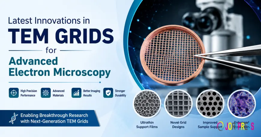
Transmission Electron Microscopy (TEM) has revolutionized materials science, nanotechnology, life sciences, and semiconductor research by enabling scientists to visualize structures at the atomic level. However, the quality of TEM imaging depends not only on the microscope itself but also on the consumables used during sample preparation. Among these, TEM grids play a crucial role in ensuring accurate imaging and reliable analytical results.
With continuous advancements in microscopy, manufacturers are developing innovative TEM grids that offer improved stability, enhanced conductivity, reduced contamination, and better compatibility with advanced analytical techniques. This article explores the latest innovations in TEM grids and how they are transforming advanced electron microscopy.
What Are TEM Grids?
TEM grids are thin, mesh-like supports designed to hold ultra-thin specimens for imaging in a Transmission Electron Microscope. They are typically made from metals such as copper, gold, nickel, molybdenum, or titanium and may be coated with support films like carbon, graphene, silicon oxide, or holey carbon.
The choice of TEM grid directly influences image quality, sample stability, and analytical accuracy.
Why Innovation in TEM Grids Matters
Modern electron microscopy demands higher resolution, better chemical analysis, and minimal sample interference. Traditional TEM grids often present challenges such as:
-
Sample contamination
-
Beam-induced damage
-
Poor conductivity
-
Mechanical instability
-
Limited compatibility with cryogenic imaging
To overcome these limitations, manufacturers continue introducing advanced grid technologies that improve imaging performance while simplifying sample preparation.
Latest Innovations in TEM Grids
1. Graphene-Coated TEM Grids
One of the most significant innovations is the introduction of graphene support films.
Graphene is an ultra-thin layer of carbon atoms arranged in a hexagonal lattice, providing exceptional electrical and mechanical properties.
Advantages
-
Nearly transparent to electron beams
-
Extremely strong and lightweight
-
Reduced background noise
-
Improved image contrast
-
Excellent electrical conductivity
These grids are especially valuable for biological imaging and nanomaterial characterization.
2. Holey Carbon Support Films
Holey carbon films have become the standard for high-resolution TEM applications.
Instead of a continuous carbon layer, these grids contain microscopic holes that allow imaging without interference from the support film.
Benefits
-
Higher image clarity
-
Reduced scattering
-
Better cryo-EM performance
-
Enhanced particle distribution
Researchers commonly use holey carbon grids for protein structure analysis and nanoparticle studies.
3. Ultrathin Carbon Film Grids
Manufacturers now produce carbon films only a few nanometers thick.
These ultrathin supports provide:
-
Improved transparency
-
Lower background signal
-
Better elemental analysis
-
Higher imaging resolution
They are widely used in analytical TEM and Electron Energy Loss Spectroscopy (EELS).
4. Gold TEM Grids for Cryo-Electron Microscopy
Gold grids have gained popularity in Cryo-EM applications.
Compared to conventional copper grids, gold grids provide:
-
Reduced beam-induced movement
-
Improved thermal stability
-
Better conductivity
-
Higher imaging precision
This innovation has significantly improved the quality of single-particle cryo-electron microscopy.
5. Silicon Nitride TEM Grids
Silicon nitride membranes are replacing traditional support films in several advanced applications.
Their advantages include:
-
Exceptional flatness
-
High mechanical strength
-
Excellent chemical resistance
-
Uniform thickness
-
Compatibility with in-situ experiments
These grids are commonly used in semiconductor research and nanotechnology.
6. Functionalized TEM Grids
Modern TEM grids now feature specially treated surfaces designed to improve sample adhesion.
Surface modifications include:
-
Hydrophilic coatings
-
Hydrophobic coatings
-
Plasma-treated surfaces
-
Chemical functionalization
These innovations improve sample distribution while minimizing aggregation.
7. Quantifoil TEM Grids
Quantifoil grids contain precisely engineered hole patterns that provide uniform specimen support.
Benefits include:
-
Consistent ice thickness
-
Better Cryo-EM imaging
-
Reduced charging effects
-
Improved reproducibility
They are among the most widely used grids in structural biology.
8. Low-Contamination Manufacturing Techniques
Manufacturers are adopting cleaner production processes to reduce contamination from oils, dust, and residues.
Advanced cleaning methods include:
-
Plasma cleaning
-
Vacuum packaging
-
Ultra-clean manufacturing environments
These innovations help maintain specimen purity and improve imaging accuracy.
9. Specialized Alloy TEM Grids
Researchers now have access to grids manufactured from specialized metals including:
-
Gold
-
Nickel
-
Titanium
-
Molybdenum
-
Beryllium Copper
Each material offers unique benefits for different microscopy applications, such as corrosion resistance, thermal stability, or magnetic compatibility.
10. AI-Assisted Quality Inspection During Manufacturing
Leading TEM grid manufacturers now use automated optical inspection systems and AI-assisted quality control to detect defects such as broken mesh, coating inconsistencies, or contamination before products reach laboratories.
This ensures:
-
Better manufacturing consistency
-
Higher product reliability
-
Fewer imaging artifacts
-
Improved reproducibility across experiments
Applications of Advanced TEM Grids
Modern TEM grids support a wide range of scientific fields, including:
-
Nanotechnology
-
Materials science
-
Semiconductor research
-
Pharmaceutical development
-
Life sciences
-
Polymer characterization
-
Battery research
-
Catalysis studies
-
Environmental science
-
Biomedical research
Choosing the Right TEM Grid
Selecting the appropriate TEM grid depends on several factors:
Sample Type
Biological samples often require holey carbon or graphene grids, while metallic samples may perform better on standard metal supports.
Imaging Technique
Different analytical methods such as Cryo-EM, STEM, EDS, or EELS require specialized grid designs.
Support Film
Choose between:
-
Carbon film
-
Holey carbon
-
Graphene
-
Silicon nitride
-
Lacey carbon
Grid Material
Common materials include:
-
Copper
-
Gold
-
Nickel
-
Titanium
-
Molybdenum
Each provides unique advantages depending on the experimental conditions.
Benefits of Purchasing TEM Grids from Reliable Suppliers
Trusted TEM grid suppliers provide:
-
Consistent manufacturing quality
-
Certified materials
-
Low contamination products
-
Wide product selection
-
Technical support
-
International quality standards
-
Fast delivery
-
Compatibility with leading electron microscopes
Working with reputable suppliers helps laboratories achieve reliable imaging results while minimizing experimental errors.
Future Trends in TEM Grid Technology
The future of TEM grids is focused on improving imaging precision while reducing sample preparation complexity. Emerging developments include:
-
Next-generation graphene support films
-
Ultra-low background grid materials
-
Smart functional surface coatings
-
Improved cryogenic compatibility
-
Nano-engineered support structures
-
Sustainable manufacturing processes
-
Greater compatibility with automated microscopy workflows
These advancements will continue to enhance high-resolution imaging and analytical performance across research and industrial laboratories.
Conclusion
TEM grids are far more than simple sample holders—they are essential components that directly influence the quality, accuracy, and reliability of electron microscopy results. Innovations such as graphene-coated grids, ultrathin carbon films, silicon nitride membranes, gold grids, and precision-engineered support structures are enabling researchers to achieve higher resolution, lower contamination, and improved analytical performance.
As electron microscopy continues to advance, selecting high-quality TEM grids from reliable suppliers will remain critical for obtaining consistent, high-resolution results in materials science, nanotechnology, life sciences, and semiconductor research. Investing in modern TEM grid technologies ensures better imaging outcomes and supports the growing demands of cutting-edge scientific discovery.
What's Your Reaction?
 Like
0
Like
0
 Dislike
0
Dislike
0
 Love
0
Love
0
 Funny
0
Funny
0
 Angry
0
Angry
0
 Sad
0
Sad
0
 Wow
0
Wow
0