3D Through-Silicon-Via (TSV) Devices Market is Projected to Reach US$ 44.93 Billion by 2033
 swatichaudhari
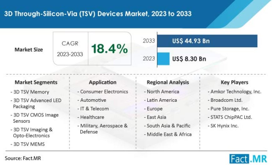

The global 3D through-silicon-via (TSV) devices market has reached a value of US$ 8.3 billion in 2023. According to Fact.MR, worldwide sales of 3D through-silicon-via devices are projected to reach US$ 44.93 billion by 2033, increasing at a significant CAGR of 18.4%.
3D TSV solutions are a type of packaging technology used in the semiconductor industry to vertically stack and interconnect multiple integrated circuit (IC) chips. TSV technology is a crucial advancement that enables the integration of three-dimensional (3D) silicon and 3D integrated circuits (ICs). It facilitates the shortest interconnections between chips and allows for the interconnection of smaller pad sizes and pitches. The stacking of chips in a three-dimensional arrangement using TSV technology has become an emerging and advanced packaging solution for memories, CMOS imagers, and MEMS.
For More Insights into the Market, Request a Sample of this Report:
https://www.factmr.com/connectus/sample?flag=S&rep_id=6959

Key Segments of 3D Through-Silicon-Via (TSV) Devices Industry Research Report
By Product : 3D TSV Memory, 3D TSV Advanced LED Packaging, 3D TSV CMOS Image Sensors, 3D TSV Imaging & Opto-Electronics, 3D TSV MEMS
By Process Realization : First Process Realization, Middle Process Realization, Last Process Realization
By Application : Consumer Electronics, Automotive, IT & Telecom, Healthcare, Military, Aerospace, & Defense
By Region : North America, Latin America, Europe, East Asia, South Asia & Oceania, MEA
TSV devices also lower power consumption due to shorter interconnects and improved heat dissipation. They support the integration of diverse technologies and materials, improving reliability.
The growth of the 3D Through-Silicon-Via (TSV) devices market is primarily driven by the increasing demand for compact and high-performance electronic devices. As consumers and industries seek smaller, more powerful gadgets, the TSV technology enables enhanced integration density and improved performance.
Implementing 3D Through-Silicon-Via (TSV) technology is challenging due to complex manufacturing processes like etching, bonding, and thinning. Etching involves precisely creating vertical vias, bonding requires accurate layer connections, and thinning reduces wafer thickness. Stacking multiple layers of devices in a small space can result in heat dissipation challenges, requiring effective thermal management solutions to prevent overheating.
Key Takeaways:
The United States market is expected to witness a CAGR of 18.9% during the forecast period (2023–2033). Moreover, the UK market is predicted to witness a market value of US $ 2.74 Bn in 2033. India and China market is predicted to witness a value of US $ 3.7 Bn and US $ 8.13 Bn by 2033 respectively.
The German market for 3D TSV devices is valued at US $ 614.1 Mn in 2023.
Increasing investments in semiconductor manufacturing initiatives are expected to contribute to the sales of devices in China. China’s market is expected to reach a market value of US $ 8.13 Bn by 2033.
Market Competition
In this competitive market, major stakeholders are dedicated to advancing 3D Through-Silicon Via (TSV) technologies, including cutting-edge packaging solutions, increased interconnect densities, and improved power efficiency. Notable companies at the forefront of these developments include Amkor Technology, Inc., Broadcom Ltd., Pure Storage, Inc., STATS ChipPAC Ltd., SK Hynix Inc., and Invensas Corporation.
In a noteworthy advancement in June 2022, Intel achieved progress in power management for chipsets within 3D stacked System in Package (SIP) designs. The company introduced fully integrated voltage regulators (FIVRs) incorporating embedded inductors.
Leading companies in the market are engaging with strategic partnerships and collaborations with other key companies including system integrators, device manufacturers, and semiconductor manufacturers.
Get Customization on this Report for Specific Research Solutions:
https://www.factmr.com/connectus/sample?flag=RC&rep_id=6959
Winning strategies
Major players in the 3D through-silicon-via (TSV) devices market is smartly focusing on creating advanced packaging solutions. These solutions use 3D TSV technology to tackle specific challenges in high-performance computing, mobile devices, and automotive electronics.’
Given the importance of memory in various electronic devices, key players might emphasize strategies that involve the vertical stacking of memory components using 3D TSV technology, catering to the demand for high-capacity and high-performance memory solutions.
As the demand for smaller and more energy-efficient devices grows in wearables and IoT, key players in the market should focus on strategies that highlight the benefits of making devices smaller. 3D TSV technology enables compact and integrated devices without compromising performance, ideal for sleek wearables.
The adoption of 3D TSV devices in consumer electronics is anticipated to experience a Compound Annual Growth Rate (CAGR) of 18.6% over the next decade.
Manufacturers of consumer electronics are actively pursuing the development of smaller, slimmer, and more compact devices. The use of 3D Through-Silicon Via (TSV) technology enables the vertical integration of components, leading to increased device density and a smaller overall footprint. By eliminating the need for traditional wire bonding or flip-chip interconnects, TSV devices contribute to significant size reduction, making them well-suited for portable devices like smartphones, tablets, wearables, and various other electronic gadgets.
Consumers now demand advanced features and capabilities from their electronic devices. 3D TSV devices play a crucial role in meeting these expectations by facilitating improved functionality through the integration of diverse components-such as processors, memory chips, sensors, and communication modules-into a single package. This integrated approach enhances device performance, supports multi-functional capabilities, and contributes to seamless user experiences.