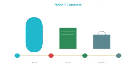


The Growing Demand for HDI PCB in Smartphones, Wearables, and IoT Devices
Get premium HDI PCB solutions from MKTPCB. Our high-density interconnect boards are ideal for smartphones, wearables, and IoT devices. Enjoy precise multilayer fabrication, fast turnaround, and competitive pricing. Request a quote today!
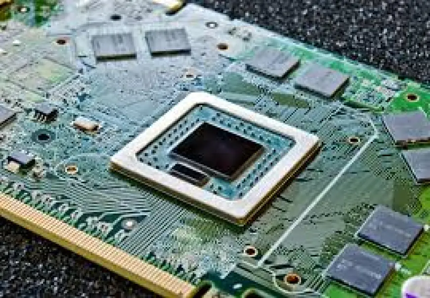
As the electronics industry continues its shift toward miniaturization, the need for compact yet high-performance circuit boards has never been greater. One technology that has become central to this evolution is the HDI PCB (High-Density Interconnect Printed Circuit Board). With their ability to accommodate more components in smaller spaces, HDI PCBs are fueling innovation across smartphones, wearables, and the rapidly expanding Internet of Things (IoT) market.
Understanding the Role of HDI PCB
HDI PCBs are a specialized class of circuit boards characterized by finer lines and spaces, smaller vias, and higher connection pad densities. Unlike traditional PCBs, they support advanced features like laser-drilled microvias, via-in-pad technology, and multiple layers of interconnects, all while maintaining structural integrity in extremely compact formats.
The HDI PCB is engineered to handle high-speed signals, improve signal integrity, and reduce electromagnetic interference—all critical factors in modern electronic design. These features make them indispensable in applications that require performance, reliability, and space efficiency.
Why HDI PCB Is Vital in Smartphones
Smartphones are one of the most complex consumer electronics on the market today. They demand:
-
High processing power
-
Compact form factors
-
Extended battery life
-
Multiple connectivity modules
-
Enhanced thermal management
To meet these demands, manufacturers rely on HDI technology. An HDI PCB allows designers to integrate more transistors, microcontrollers, antennas, and memory units into limited space, enabling sleeker designs without sacrificing performance.
Additionally, HDI boards support blind and buried vias, reducing the number of layers needed and improving signal transmission. The result is a faster, more energy-efficient device that still fits comfortably in your pocket.
The Influence of HDI in Wearable Technology
Wearables, such as fitness trackers, smartwatches, and health monitors, are defined by their need to be lightweight, compact, and durable. These devices often integrate GPS, heart rate sensors, wireless connectivity, and battery modules—all in form factors smaller than traditional electronics.
Here, HDI PCBs shine by enabling multilayer routing in limited space. Their thin profile and high routing density are key advantages in wearable applications. Plus, their capability to support rigid-flex designs makes them suitable for devices that must bend or flex to fit the body comfortably.
Manufacturers can also use HDI technology to improve water resistance and mechanical stability—two critical qualities for any wearable product.
IoT Devices and the HDI Advantage
The IoT ecosystem—spanning smart homes, industrial automation, medical monitoring, and agriculture—is built on compact and energy-efficient embedded systems. These devices often operate remotely, collect data, and communicate with networks wirelessly.
An IoT device needs to be:
-
Small and discreet
-
Reliable over long operational periods
-
Capable of wireless communication
-
Resistant to environmental factors
HDI PCB enables the miniaturization of these devices without compromising performance. Whether it’s a smart thermostat, security camera, or connected medical sensor, HDI boards offer the essential high-density wiring and component placement needed to support IoT functionality in small packages.
Manufacturing Benefits of HDI PCB
Apart from the technical benefits, HDI PCBs offer practical advantages to manufacturers:
-
Fewer layers required: Efficient layout and interconnectivity reduce the total number of PCB layers.
-
Improved signal performance: Shorter trace lengths and controlled impedance enhance signal integrity.
-
Lower overall system cost: While HDI fabrication can be more expensive, the resulting design often reduces total component count and assembly complexity.
-
Faster time to market: HDI technology supports rapid prototyping of compact and multifunctional devices.
These benefits directly contribute to more competitive product development cycles, which is especially important in fast-moving consumer electronics markets.
Design Trends and Future Outlook
With technologies like 5G, AI chips, and edge computing becoming standard in mobile and IoT devices, the demand for advanced PCB designs will only increase. HDI PCBs will continue to play a vital role in enabling more intelligent, compact, and connected electronics.
Designers are also increasingly turning to flex-HDI PCBs, which combine the benefits of flexible circuits with HDI features. This is particularly relevant for foldable smartphones, medical wearables, and smart clothing.
Environmental sustainability is another emerging factor. Because HDI boards can reduce material waste and use fewer interconnects, they may contribute to greener electronics manufacturing practices in the future.
Final Thoughts
The technological push toward smaller, faster, and more functional devices has placed HDI PCBs at the forefront of electronics innovation. From the sleek smartphone in your hand to the smartwatch on your wrist and the smart sensor in your home, these boards enable the form and function that modern users expect.
As industries continue to demand higher performance in tighter spaces, it’s clear that HDI PCB technology will remain essential—not just in smartphones, wearables, and IoT devices, but across the entire landscape of connected electronics.
What's Your Reaction?
 Like
0
Like
0
 Dislike
0
Dislike
0
 Love
0
Love
0
 Funny
0
Funny
0
 Angry
0
Angry
0
 Sad
0
Sad
0
 Wow
0
Wow
0