Glass Wafer for Semiconductor Devices Market Analysis, Size, Share, Growth, Trends, and Forecasts by 2031
As semiconductor technology advances into smaller feature sizes and innovative device architectures, glass wafers must keep pace.
 Punam
Punam

Within the Glass Wafer for Semiconductor Devices market, the industry dynamics are driven by the demand for increasingly smaller and more powerful electronic components. As technological innovation propels the semiconductor sector forward, glass wafers become pivotal in enabling the production of smaller and more efficient semiconductor devices. This market thrives on the perpetual quest for miniaturization and enhanced performance in electronic applications. Glass wafers are an integral component in the production of semiconductor devices like integrated circuits, transistors, and diodes. The silicon semiconductor industry relies heavily on high-quality glass wafers to provide a stable base for manufacturing chips and circuits.
???????????? ???? ???????????????? ???????????????????????? ????????????????????????:https://www.metastatinsight.com/request-sample/2580
Top Companies
Corning Inc.
Asahi Glass Co., Ltd
Plan Optik
Tecnisco Ltd
Nippon Electric Glass Co., Ltd.
Samtec
Dsk Technologies Pte Ltd
Swift Glass Inc.
Nano Quarz Wafer
SCHOTT AG
WaferPro LLC
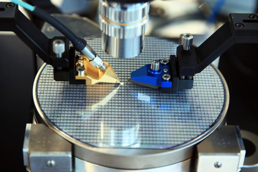
The glass wafer begins as a cylindrical boule made from materials like quartz, borosilicate glass, or aluminosilicate glass. These glass formulations possess high uniformity and chemical stability needed for fabricating electronic components. The boule is sliced into thin discs using specialized saws, then polished down to an optically flat and scratch-free surface. These glass wafers serve as the foundational substrate onto which the active layers of a semiconductor device are deposited.
Access Full Report @https://www.metastatinsight.com/report/glass-wafer-for-semiconductor-devices-market
Before device fabrication, glass wafers undergo extremely thorough cleaning and surface preparation. Steps like solvent cleaning, wet chemical etching, and high temperature annealing remove contaminants and enhance the molecular bonding between the glass and deposited films. The purity and integrity of the glass wafer surface is paramount for enabling proper electrical performance and reliability.
The semiconductor layers such as dielectric insulators, conductors, and photoresist are laid down on the wafer through techniques like molecular beam epitaxy, chemical vapor deposition, sputtering, and lithography. The glass provides mechanical support while these overlying materials are patterned and etched into integrated circuits or discrete components. The flatness and stability of the wafer surface facilitates precision patterning down to nanometer dimensions.
Glass offers key advantages over other wafer materials for electronics manufacturing. It is inexpensive, nonconductive, and optically transparent. The thermal expansion coefficient and melting point of glass pairs well with silicon. Glass allows inspection and metrology of circuits using optical transmission. And glass wafers are easily scaled up to accommodate larger generation chip sizes and increased production volumes.
As semiconductor technology advances into smaller feature sizes and innovative device architectures, glass wafers must keep pace. Manufacturers continually refine glass composition, surface quality, and mechanical strength to meet industry demands. Investment in glass wafer engineering aims to bolster chip yields, processing capabilities, and end-product performance.
With its unique set of chemicals, optical, thermal, and mechanical attributes, glass remains an indispensable material at the heart of modern semiconductor fabrication. As the foundational substrate for microelectronics, the humble glass wafer enables our interconnected digital world of computers, appliances, mobile devices, and cutting-edge electronics.
Global Glass Wafer for Semiconductor Devices market is estimated to reach $470.6 Million by 2031; growing at a CAGR of 5.5% from 2024 to 2031.
Contact Us:
https://www.metastatinsight.com
inquiry@metastatinsight.com
+1 214 613 5758